The network analyzer can provide full functionality for high-speed digital data structure testing on PCB. In addition, the de-embedding method can eliminate errors from the sensing head, probe, and capacitance pin to connect to the signal line. In this article, we will learn about the TDR measurement solution.

With continuously increasing data rates, the signal integrity aspects of high-speed digital designs and the components used are becoming increasingly complex. Especially at higher data rates, vector network analyzers (VNA) are gradually replacing traditional time domain reflectometry (TDR) setups for examining passive elements, such as connectors, cables, PCB, etc. The applications and conveniences of using VNA make VNA the chosen device in the field.
Purpose:
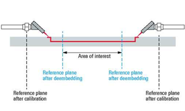
When performing tasks such as verifying high-speed signal structures on a PCB, measurements must be implemented on specific layers without the impact of probes, converters, etc. It requires using precise de-embedding algorithms to calculate and remove these effects from the measurements, leaving only the results for the region of interest.

Measurement solution:
The setup below shows an example to verify high-speed differential signals on PCB up to 20 GHz.
The device used is a 4-port VNA vector network analyzer. Common de-embedding tools such as (Delta-L, EMStar Delta-L+, EMStar Smart Fixture De-embedding (SFD), or AtaiTec In-Situ De-embedding (ISD) can be run directly on the machine, without the need for an additional external one.
Automated Implementation Process
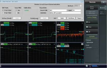
To simplify this process and guide the operator through the test steps, testing is often automated through software. The screenshot on the left shows an example of the three stages of this test procedure:
- Measure the two short-circuit terminals to calculate the error (de-embedding).
- Measure the entire circuit to be tested.
- Calculate the results of the area to be measured based on the de-embedding method.

Eye Diagram

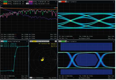
To meet some advanced needs, the network analyzer can be used to analyze the lattice plot of the test data area. This feature allows users to evaluate signal quality, such as amplitude noise, time-domain chaos, etc. In addition, it can also set up a mask test to quickly assess PASS/FAIL results.
Our company always wishes to become a reliable partner and a leading supplier of equipment and solutions for the success of our customers. For more detailed information, please contact:
MITAS Hanoi Technology JSC
Address: 5th Floor, C’Land Building, No. 81 Le Duc Tho St., My Dinh 2 Ward, Nam Tu Liem Dist., Hanoi, Vietnam
Web: https://mitas.vn | Tel: (+84) 243 8585 111 | Email: sales@mitas.vn
The trust and support of our customers are a driving force and an invaluable asset to our company. We sincerely thank you./.

